PROJECT
Realizing Co-Packaged Optics technology! Photonics connecting the future
Top / Research and Development / Towards the realization of Photonics-Electronics-Convergence technology! A future connected by light /The Importance of Optical Waveguides and On-Board Optical interconnects | Technology for Next-Generation Data Centers
Copied to clipboard
What is the optical waveguide technology that supports high-speed, low-latency optical communications?
As the demand for high-speed data communication in data centers and high-performance computing (HPC) fields rapidly increases, **Optical Waveguides** have become an essential technology. In particular, **On-Board Optical Interconnects** are attracting attention as a next-generation communication technology that utilizes Silicon Photonics. In this article, we will explain the basic concept of optical waveguides, the latest technology, and Hakusan's optical waveguide solutions.
What is an optical waveguide? - Role and advantages of on-board Optical Interconnect-
Fundamentals of Optical Waveguides
Optical waveguides are made of optical materials designed to transmit optical signals along specific paths, and offer significant advantages over conventional electrical wiring, including low latency, low loss, and high bandwidth.
Advantages of Optical Waveguides
- Ultra-high-speed data transmission: Optical signal transmission of over 100 Gbps possible
- Low power consumption: More energy efficient compared to electrical wiring
- EMI (electromagnetic interference) free: Less susceptible to radio interference, ensuring stable communication
- Miniaturization and high density: Combination with silicon photonics technology enables even more highly integrated data communication
Manufacturing technologies and types of optical waveguides
Optical waveguides are manufactured using the following technologies:
- Photolithography: Forming fine optical waveguides on a silicon substrate
- Imprint method: Creating low-cost, high-precision optical waveguides using polymer materials
- Mosquito Method:
3D polymer optical waveguide formation technology (developed by Ishigure Laboratory, Keio University)
Utilizing on-board Optical Interconnect and silicon photonics
The importance of on-board Optical Interconnect
With conventional electrical wiring, signal degradation becomes noticeable when data speeds exceed 100 Gbps, and increased power consumption becomes an issue. Utilizing technologies such as **Co-Packaged Optics (CPO) and On-Board Optics (OBO)** makes it possible to use Optical Interconnect within the board, which is expected to improve power efficiency and bandwidth.
Combining silicon photonics and optical waveguides
Silicon photonics is a technology that utilizes semiconductor process technology to integrate optical waveguides and electronic circuits, and is an essential element of next-generation data centers and AI infrastructure.
Main application areas
- Internal cabling of data centers (Optical switching, optical fiber connections)
- Optical communication between AI accelerators (Low-latency, high-bandwidth optical interconnection)
- Photonic Quantum Computing (Waveguide Technology for Quantum Communication)
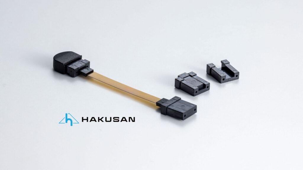
Hakusan 's Optical Waveguide Technology | PMT Connector and Mosquito Method
PMT connectors and optical waveguide films
Hakusan has achieved high reliability for on-board Optical Interconnect by utilizing PMT connectors. This connector, combined with optical waveguide film, enables narrow-pitch, low-loss Optical Interconnect.
The PMT connector has a similar shape to MT Ferrule, a key component in multifiber optical connector, and is highly compatible with MT Ferrule.
This feature enables seamless connection between optical waveguides and optical fibers, enabling high-speed, low-loss optical communications.
Optical waveguide formation using the Mosquito method
Hakusan is collaborating with Keio University to develop three-dimensional optical waveguides using the Mosquito method. This technology has the following advantages:
- High density mounting: Narrow pitch Optical Interconnect is realized.
- Edge coupling support: Connection between silicon photonics chip and optical fiber is possible.
- 3D Optical Interconnect: It is possible to wire in the vertical direction between multilayer boards and chips, overcoming the limitations of conventional 2D Optical Interconnect design.
The Mosquito method uses a dispenser and a multi-axis robot to create optical waveguides of any shape. In particular, by combining it with narrow pitch and edge coupling technology, it is possible to achieve even higher density wiring within the board.
summary
Optical waveguide technology is a key technology for achieving low latency, high bandwidth, and low power consumption in data centers and AI infrastructure. In particular, combining it with silicon photonics technology will overcome the limitations of conventional electrical wiring and make it possible to build new communication infrastructure. Hakusan is developing next-generation in-board Optical Interconnect technology using PMT connectors and the mosquito method.
We will continue to innovate in the future as a partner that provides optimal optical waveguide solutions to companies that handle optical circuit boards and other products.
Useful links
・Mosquito Method / Takaaki Ishigure (Info-Optics Laboratory)
Copied to clipboard
Upon request, we can share research and development information and provide samples.
Please feel free to contact us.